A new design of a lab-grade data logger has been developed using a PIC microcontroller and a 20-bit delta-sigma converter. The data logger provides 8-channel DC inputs and the optional digital inputs. The sampling interval can be programmed from 1min to 1Hr. The device uses a cheap memory card for data storage. In addition, the optional serial port also provides data stream for displaying real-time signal on the terminal.
1. Introduction
The new data converter technology using delta-sigma simplifies the design of high resolution data recording device. One of the interesting chip is Linear Technology LTC2400, 24-bit ADC. Some of my designs were used this converter. Another chip of interest is LTC2420, 20-bit ADC. The chip has pin and data output compatible to the LTC2400. I design the new data logger using the LTC2420 and use the cheap memory card for data storage.

Figure 1: G5 Data Logger enclosed with standard 145x145x80mm plastic box.
2. Hardware description
The hardware schematic is shown in Figure 2. The microcontroller is the PIC18F45K20. The package is 40-pin PDIP. The chip runs with a 2MHz internal oscillator. The HS oscillator connected to OSC1 and OSC2 is optional. The low power oscillator using a 32,768Hz crystal is connected to RC0 and RC1. RC7 and RC6 are TTL level UART interface. It provides 9600bit/s data stream for connecting the PC. The SPI port, RC3/SCK, RC4/SDI and RC5/SDO are used to interface the memory card in SPI mode through the J2 memory card socket. RD5, RD6 and RD7 are software controlled SPI port for interfacing the delta-sigma converter, U5 LTC2420. D2 is a bandgap reference diode providing 1.2Vref for the analog to digital converter U5. The analog input multiplexer uses CMOS analog switch,U3 CD4051. CH1 to CH4 are 1V full scale. CH5 to CH8 are 10V full scale. CH5 to CH8 use the input voltage divider. The real-time clock is provided by U4, DS1302. BT1 is a super capacitor 0.33F for power backup to the RTC chip. The DS1302 is programmed to provide tickle charge to the BT1. U9 is TTL to RS232 converter using MAX3232. The power supply provides +5V and +3.3V logic. All logics are used +3.3V. The +5V is for sensor interfacing. The voltage regulators are fixed output linear regulators, LM1117, U7 for +3.3V and U8 for +5V. J7 is for dry cell battery connector. The recommended battery is +6V 2.8AH dry cell battery. U6 is current regulator built with LM317 and R19. It provides the battery charging current from the DC sources, i.e. AC adapter or small solar cell panel. The charging current is computed by 1.25V/Icharge.

Figure 2: Hardware schematic.
2. Prototype
The PCB board is double layer. Figure 3 shows the component layer, the center chip is PIC18F45K20.

Figure 3: Component layer.
The bottom layer or soldering side is for input terminal and the memory card socket.

Figure 4: Bottom layer.
3. Analog input terminal
The analog input terminal is screw type. CH1-CH4 accepts 0-1VDC and CH5-CH8 for 0-10VDC single end input. Pin 16 provides +5V for sensors interfacing. The reading resolution for CH1-CH4 is 1 microvolt, and 10 microvolts for CH5-CH8.

The optional digital input signals is the bottom row terminal.

Each pin has its functional as described below.
Pulse counter=TTL1 (CH16)
Frequency counter=PULSE2 (CH17)
Logic input=TTL1 (CH13)
Logic input=TTL2 (CH14)
Logic input=TTL3 (CH15)
TTL1, TTL2 and TTL3 can be used to monitor the contact status between 0V or +12V input. The value "1" shown in the record means +12V input and value "0" for 0V input.
For pulse signal, TTL1(pin4) accepts the TTL pulse. The counter for CH16 is 32-bit totallizer.
For frequency measurement, PULSE2 (pin2) accepts TTL signal with frequency from DC to 15kHz. The reading is +/-1Hz.
The digital terminals also provide optional 10-bit resolution ADC for 0-3VDC input at AN1(CH9), AN2(CH10), and AN3(CH11).
CH12 is battery voltage monitored by internal firmware
4. Using the Analog Device TMP36, Celsius temperature sensor with G5-Data Logger
The TMP36 is an integrated circuit designed for measuring temperature from -40C to +125C. It provides DC output that is linearly proportional to the Celsius temperature unit. The chip do not require any external calibration to provide accuracy's of +1C at 25C and +2C over -40C to +125C.

The relationship between output voltage and Celsius temperature is,
Temp in °C = (Vout – 0.500 ) x 100
For example at 25C, Vout will be 0.750V. At -40C, Vout will be 0.100V. We can use above equation for converting the reading in Volt to Celsius unit easily.
The package of TMP36 is TO-92 plastic. It has 3-pin, VCC, Vout and GND. For VCC we can use +5V provided at the analog input terminal. Vout can tie to a given analog input directly.
5. Specifications
Number of analog input: 4-channel 0-1VDC, 4-channel 0-10VDC.
Digital input: 3-channel TTL, 1-ch pulse, 1-ch frequency
Controller: nonowatt CMOS microcontroller
Clock: super capacitor backed up RTC chip
Reading interval: programmable 10s to 1Hr
ADC: 20-bit Delta-sigma technology
Storage capacity: up to 2GB
File format: FAT
Record type: CSV, spreadsheet compatible
Power supply: +6V 2.8AHr dry cell battery (approx. 10 days logging)
Dimension: 145x145x80mm (WxLxH)
6. Download
Schematic, Firmware, Quick start, Brochure, Sample record of TMP36
K6 version with RS232 port

Figure 6: The modified version, K6 provides the RS232 port for sending real-time data to the PC.
Here is the additional circuit for the K6 version. The simple RS232 logic translation from +3V positive logic to the RS232 logic.
![]()
Figure 7: Simple RS232 logic translation with BC557.
The small program, PuTTY is used to capture and display the data sent from the data logger.
To capture data stream, select Session-Logging and mark at the Printable output. The sample log file name, putty.log is shown below.
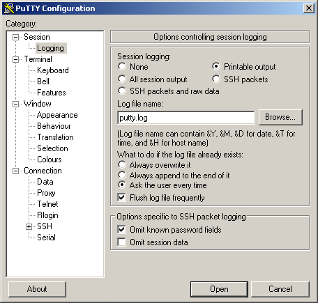
Now select Session, click at the Serial and type the COM port, shown the COM2. Then click OPEN.

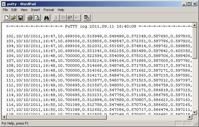
The terminal screen will show. When the reading is saved to the memory card, it will send to the serial port as well. On the terminal screen we can see the real-time data stream. This data streams are composed of ASCII code, or printable output, so it will be saved in the log file concurrently.

And here is the sample log file content. The contents are comma separate value, CSV, so it can be imported into a spreadsheet software easily.
7. Download
Contact Information
Wichit Sirichote
Department of Physics
Faculty of Science
King Mongkut's Institute of Technology Ladkrabang
Bangkok 10520 THAILAND
E-mail: wichit.sirichote@gmail.com
<