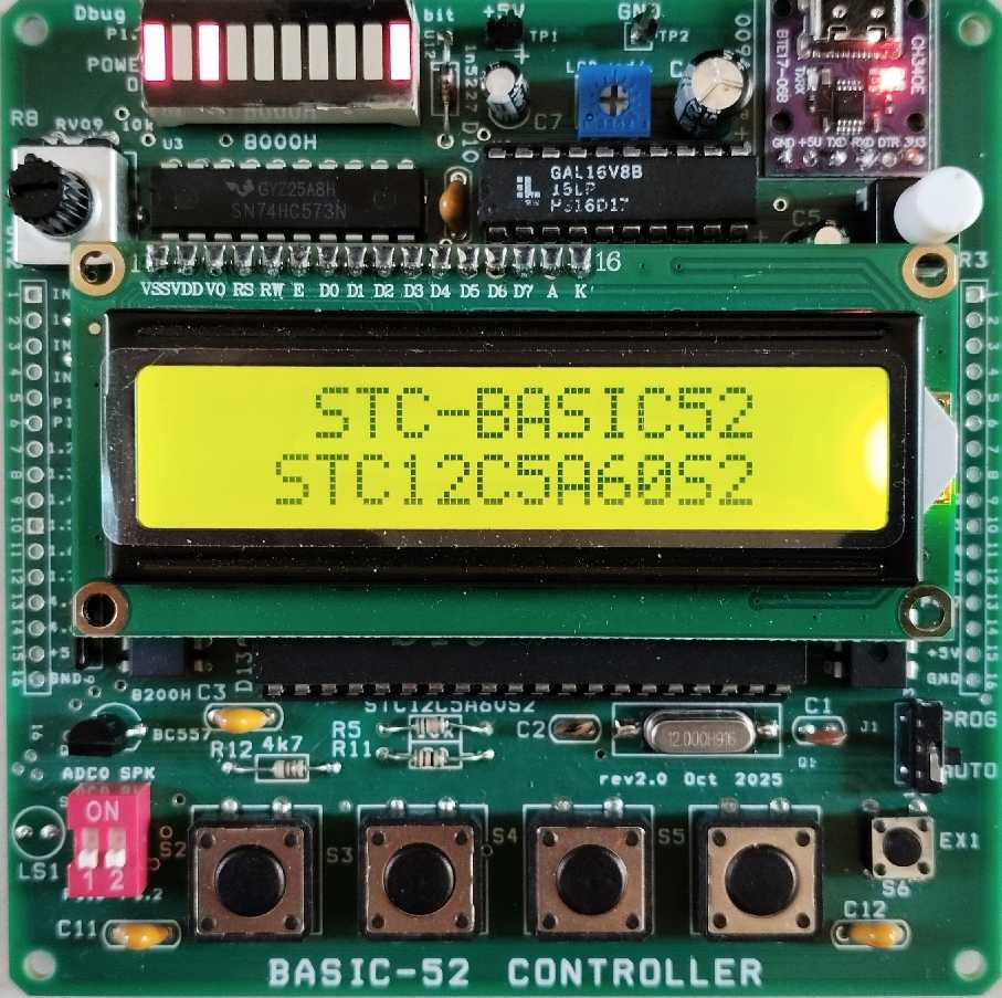
New design BASIC52 controller using STC12C5A60S2 single cycle 8051 compatible microcontroller and Ferro-electric memory. Available now, latest BASIC52 with LCD driver.
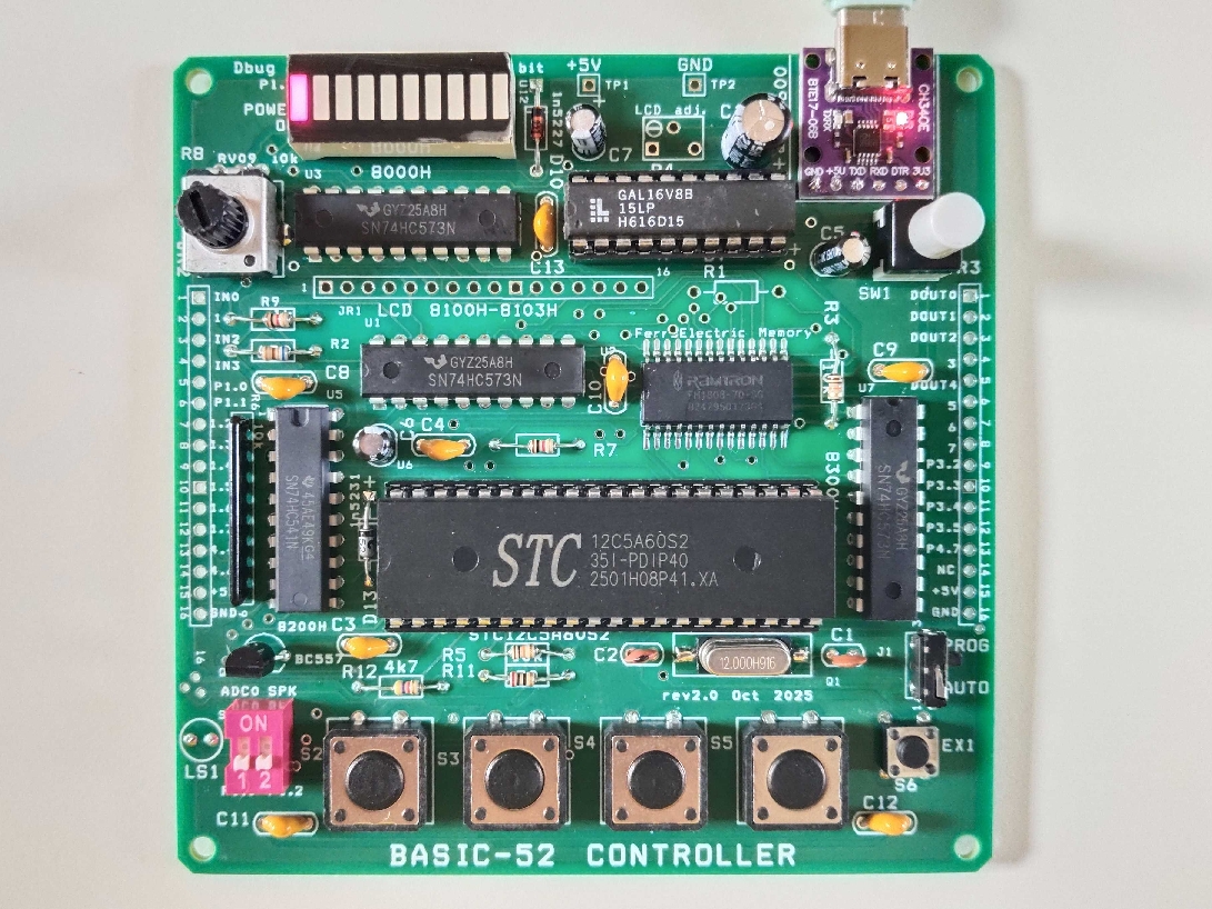
The new design BASIC52 controller is built with STC12C5A60S2, single-cycle 8051 compatible chip and a 32kB Ferro-electric memory. The controller board has preloaded the BASIC-52 interpreter with add-on functions for full access of STC's special function registers. The kit has an extra input port and output port, an RV09 pot for 0-5V analog test signal, a 10-bit bar display, and an optional text LCD port. The BASIC program can run with simple mode switch, when set to AUTO the program will start run after power on easily.
Hardware
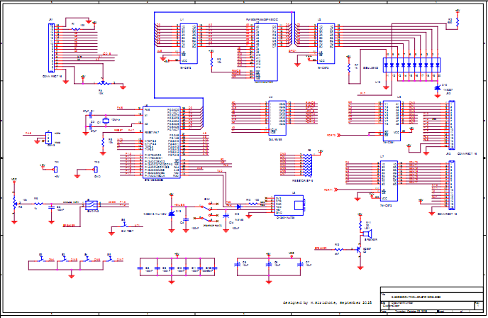
The main MCU, U6 is the STC12C5A60S2, a 40-pin DIP package, running with 12MHz xtal. The external memory chip, U2, is 32kB RAM FM1808, Ferro-electric memory. The memory and I/O space allocation are provided by PLD chip, U4 GAL16V8. U3 74HC573 is an onboard GPIO1 LED. U5 74HC541 is an 8-bit digital input port, the lower 4-bit is available at SIP connector, the upper 4-bit is tied to the onboard push button switches, S2, S3, S4 and S5. U7 74HC573 is an 8-bit digital output port, all 8-bit port are available at JR3 SIP connector. The board is powered with +5V from a USB port.
Hardware Features
MCU: STC12C5A60S2, 60kB Flash with BASIC52 interpreter
Memory: 32kB Ferro-electric RAM
Input/Output: 8-bit output port, 4-bit input port
Onboard display: 8-bit bar display, Text LCD (optional)
Onboard key switch: 4 switches push button
ADC: 10 bit, P1.0 to P1,7
Mode selector: AUTO and PROG
USB port interface
I/O locations
Location |
Port type |
Examples |
8000H |
8-bit GPIO1 |
XBY(8000H)=0FFH |
8100H-8103H |
LCD registers |
XBY(8100H) |
8200H |
8-bit Input port |
A=XBY(8200H) |
8300H |
8-bit Output port |
XBY(8300H)=B |
P1.0-P1.7 |
8-channel ADC or Digital I/O |
PORT1=255 |
P3.2-P3.5 |
4-bit 8051 port |
PORT3=255 |
P4.7 |
1-bit 8051 port |
SFR direct access |
P3.0-P3.1 |
9600 UART |
CH340 USB converter |
P4.6 |
Mode selector |
Program or Auto run mode |
Quick start with BASIC52
The controller board uses 9600 terminal for BASIC program writing. The kit is preloaded with an LED running program.
To enter PROG mode, select J1 position for PROG, the Press SW1 to reset the kit.
Type list command, to list the program.
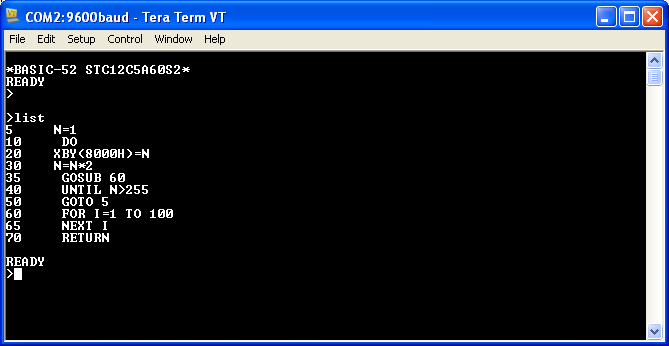
The program is very simple to understand.
Variable N is loaded with 1.
Then write to GPIO1 LED at location 8000H using XBY(8000H) command.
Update the variable by left shift one bit.
Pause some delay by calling subroutine 60
Then repeat the loop.
Loading BASIC program
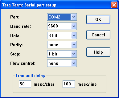
BASIC programs can be written in any PC editor. To load the program, set a delay for character 50ms and line delay of 100ms. Then click File Sending.
Here is the sample program for testing program running.
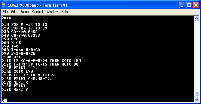
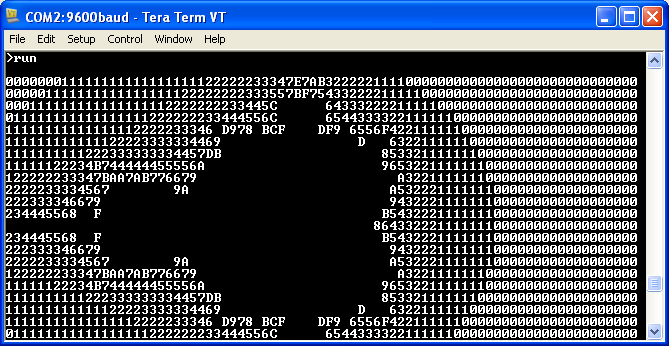
The running output is shown below.
ADC Testing program
The STC12C5A60S2 chip has a built-in 10-bit ADC converter. The ADC inputs use P1.0 to P1.7 for 8-channel analog input.
The kit has RV09 POT for ADC testing at P1.0. S1 selector channel1 selects between P1.0 digital I/O or Analog input signal. To test ADC with the onboard RV09 POT, select the ADC0 position.
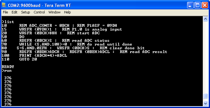
This program demonstrates how to access the STC12x chip's special function registers.
Adjust the RV09 POT, the readings will be changed from 0 to 1023.
LCD driver
The latest BASIC52 has the LCD drivers written in assembly code. The examples of LCD functions, e.g. initialize, set cursor position, clear screen are shown in the source code. The code starts at location 3000H. In the BASIC program, we can use the CALL statement to call an assembly subroutine.
The print @ is added at location 403CH. It will print any texts on LCD screen.
The example of printing an LCD program is shown below.
10 CALL 3000H : REM init LCD
|
First we call subroutine at location 3000H, to initialize the LCD interface. Then set bit 7 of internal memory at 24H, to enable print @ statement.
Line 30 sets the cursor position to line Y=0, X=3. Then line 40 prints the text on screen.
Line 50 sets the cursor to line Y=1 (2nd line), X=2. Then print text on screen.
Here is the result.
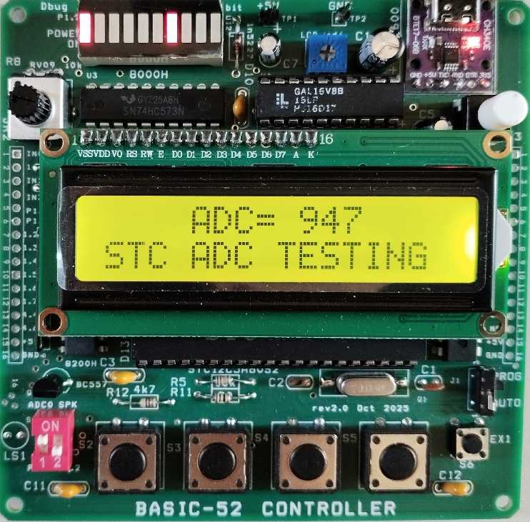
Another example is to print the ADC readings on LCD.
|
The STC12C5A60S2 chip has an 8-channel 10-bit ADC. The kit provides a voltage source of 0-5V adjustable using the R8, POT and S1 selectors.
The ADC registers can be accessed using the add-on assembly code written by H.-J. Boehling & D. Wulf.
The main program sets the ADC power and starts conversion. When completed, the ADC results are read. The result is printed on the LCD using a print @ statement.
Here is the running result. When we adjust the POT, we will see the readings changing from 0 to 1023.
How to update the BASIC52
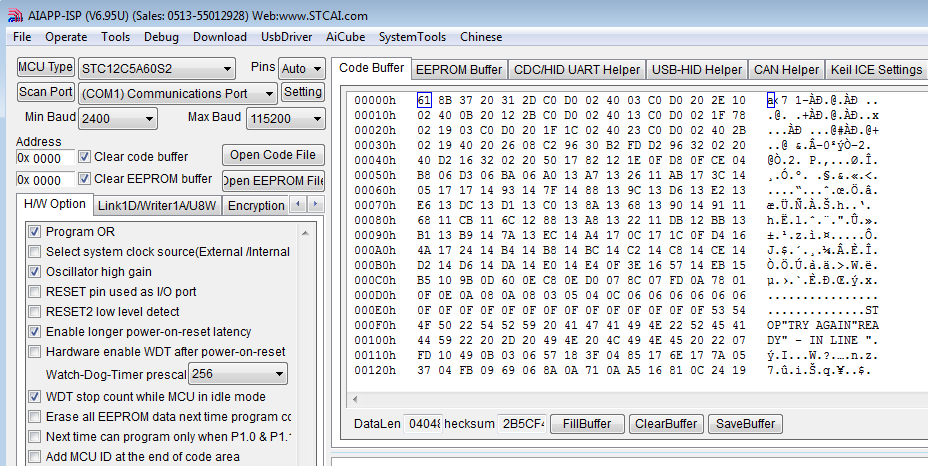
The BASIC52 software can be updated easily using the STC-ISP program.
Select the chip to STC12C5A60S2. Load the latest hex file. Click download and recycle the kit power with SW1 press and release.
PARTS LIST Semiconductors U1,U3,U7 74HC573 D10 1N5227 R1, R10 100 Capacitors C1,C2 27pF, ceramic capacitor Additional parts JR1,JR2,JR3 CONN RECT 16 |
Download
Hardware schematic, BASIC52 and BASIC test programs , PLD file , STC12C5A60S2 Datasheet, FerroElectric Memory
What's New
12 January 2026, updated BASIC52 with LCD driver.
More technical information, please contact Wichit Sirichote, wichit.sirichote@gmail.com
Last updated January, 2026
October 2025