Wichit Sirichote, wichit.sirichote@gmail.com
Build a single board microcomputer with 6502 CPU. Simple design and cheap, everyone can build it. Updated monitor is available for download now!
Back to 1982, when I was a student, I have learned the Z80 CPU with Multitech MPF-1 Kit. At the same time, I also have played with Apple II that uses 6502 CPU. But here in Thailand, Z80 is very popular. Many single boards computer use Z80 as a CPU. Colleges and university also teach basic microprocessor with Z80. I got two chips of 6502 CPU two years ago. At the yearend of 2014, 32 years since I was a student, I picked the 6502 CPU and designed the microcomputer kit again with HEX key and 7-segment display. I wrote the monitor program using 6502 instructions. I used TASM assembler. My intention is to design the microcomputer board that uses 6502 as a CPU. The kit is suitable for today student to learn many addressing modes and hardware of the 6502 CPU. The circuit is simple and easy build.
 |
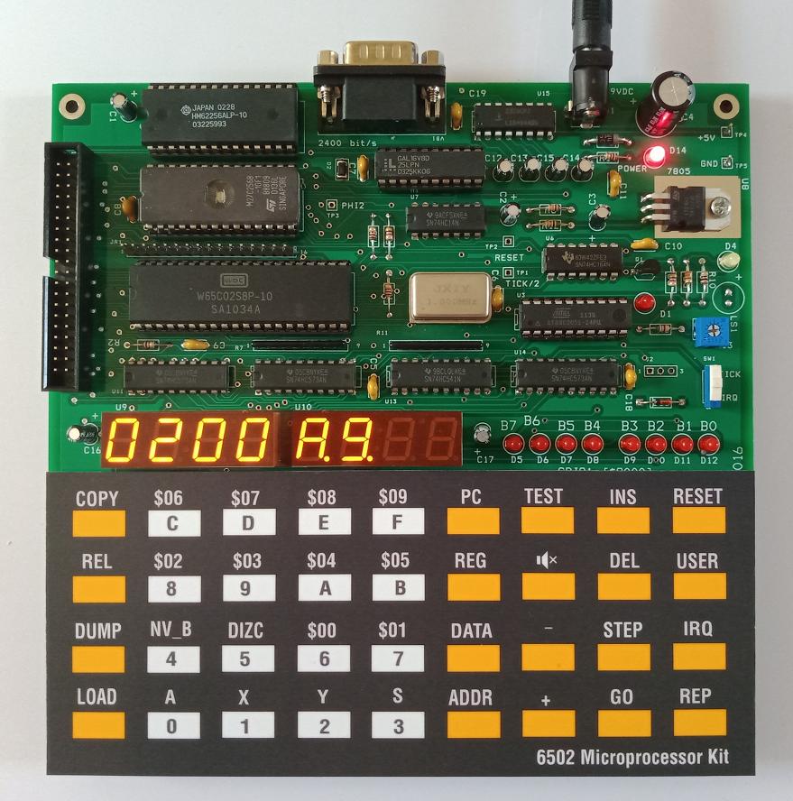
| Figure 1: 6502 Microprocessor kit |
A simplified block diagram of the 6502 Microprocessor kit is shown in Figure 2. Main parts are 6502 CPU, memory chips EPROM and SRAM. EPROM stores the monitor program and SRAM stores the variables and stack memory. The memory and I/O spaces are selected by PLD decoder. The oscillator is 1MHz. I used CMOS latch, 74HC573 as the output port and tri-state buffer, 74HC541 as the input port. The display for address and data is 6-digit 7-segment LED. Input device is hex keypad. The extra circuit, 100Hz tick generator is for experimenting with time trigger programming.
 |
| Figure 2: 6502 Microprocessor Kit block diagram. |
Hardware description: U5 is CMOS 6502 CPU. The CPU clock 1MHz is produced by oscillator module Y1-OSC-1M. U1 is 32kB EPROM, 27C256. The address space for EPROM is decoded at 0xC000-0xFFFF, where the RESET, IRQ and NMI vectors are located. U2 is 32kB static RAM, 62256. The RAM space is located at 0x0000-0x7FFF. Zero page is located at 0x0000-0x00FF and the stack memory at 0x0100-0x01FF. User program can be tested from address 0x0200. U4, memory space decoder chip made by GAL16V8D. It provides chip selected signals for memory and I/O chips. U6 is shift register used for single instruction execution. SYNC pulse that indicates instruction fetch cycle will shift the logic high from input pin at the 8th instructions. This logic high will be inverted to produce NMI signal to interrupt the CPU. User instruction will be executed once and NMI will be serviced.U3, the 20-pin 89C2051 microcontroller chip produces 10ms tick. SW1 selects between 10ms tick or manual IRQ button.
U13, 74HC541 is 8-bit input port (PORT0). Six bits, PA0-PA5 are input signals of the row keypad. PA6 is user key for repeat function. A8 pin is RxD pin of 2400 bit/s software controlled UART. U11, 74HC573 is 8-bit output port (PORT2). The 8-bit output drives the 7-segment LED directly. No current limit resistor. U12 (PORT1) drives 6-digit common cathode pin. The brightness is controlled by PWM. PC7 shares both speaker output for beep signal and TxD pin for 2400 bit/s UART. PC6 controls single step operation.
U14, 74HC573 is 8-bit output port for 8-bit binary number display. D13 lifts the forward biasing for proper brightness. J11 is 20-pin socket for text LCD interface. U15, MAX232 converts TTL level to RS232 level.
 |
| Figure 3: Hardware schematic (click to enlarge). |
PLD equations : U4 is a PLD chip used to select the memory and I/O ports. The address and I/O space can be programmed using PLD equations. The source file of PLD equations is shown in Figure 4. The PLD compiler is WinCupl. The output file, JEDEC will be used to program the PLD chip by a PLD programmer.
| Name 6502KIT ; PartNo 16V8 ; Date 12/1/2014 ; Revision 01 ; Designer Engineer ; Company Fangkhao ; Assembly None ; Location ; Device g16v8a; /* *************** INPUT PINS *********************/ FIELD ADDRESS = [A15..A12]; /* *************** OUTPUT PINS *********************/ /************** equations *************************/
!RAMCE = ADDRESS:[0000..7FFF]; !RAMWR = !RW & PHI2 & ADDRESS:[0000..7FFF]; !LCD_E = !PHI2 # !A15 # A14 # A13 # !A12; PORT0 = !RW # !PHI2 # !A15 # A14 # A13 # A12 # A1 # !A0; !PORT1 = RW # !PHI2 # !A15 # A14 # A13 # A12 # !A1 # A0; !PORT2 = RW # !PHI2 # !A15 # A14 # A13 # A12 # !A1 # !A0;
|
| Figure 4: PLD equations. |
10ms System Tick: U3,8051 compatible microcontroller is used to generate 10ms tick. The circuit runs with 6502 clock, PHI2. The tick signal is output at P3.7. TP1 is 50% duty cycle with frequency of tick/2. D1 is for indicating tick signal. Calibrating the correct tick frequency can be done by testing the pulse frequency at TP1.
 |
| Figure 5: 10ms tick generator built with AT89C2051 microcontroller. |
The source code was written in assembly code. TxD pin is available for user experiment with commands receiving from 6502. The sample below is fixed frequency 100Hz or 10ms tick.
; 10ms system Tick TIMER CHIP FOR 6502 KIT
$mod52 dseg at 30h TICK: DS 1 cseg at 0
jmp main
org 00bh timer0_vector: JMP timer0_SERVICE
org 100h ;-----initialize data----------------------------- main: mov r7,#0
djnz r7,$ mov sp,#60h ; set stack pointer to 60h MOV P1,#0FFH
MOV TICK,#0 mov tmod,#1 ; set timer mode 1
setb et0 ; enable timer0 interrupt
setb ea ; enable all interrupt
setb tr0 ; run timer0 SJMP $ ; RELOAD 0FCBFH FOR 10ms INTERRUPT TIMER0_SERVICE:
PUSH ACC
ORL TH0,#0FCH ; reload initial value
ORL TL0,#0BFH ;
CLR P3.7 ; produce interrupt trigger to IRQ
NOP ;
SETB P3.7 ; CPL P1.6 ; CHECK TICK FREQUENCY INC TICK MOV A,TICK
CJNE A,#100,SKIP
MOV TICK,#0
Clr P1.7
MOV R7,#30
DJNZ R7,$
SETB P1.7 SKIP: POP ACC
RETI |
| Figure 5: Source code listing of 10ms tick generator. |
Hardware specification:
1. CPU: 65SC02, CMOS 8-bit @1MHz clock
2. Memory: 32kB RAM, 16kB EPROM
3. Decoder chip: GAL16V8 PLD
4.
Display: 6-digit 7-segment LED
5
. Keyboard: 36 keys
6
. RS232 port: 2400 bit/s
7
. Debugging LED: 8-bit GPIO1 LED
8
. SystemTick: 10ms tick
9. Text LCD interface: direct CPU bus interface text LCD
10. Expansion header: 40-pin header
Software description: Monitor program was written with 6502 instructions. The source code are assembled to hex code using TASM assembler. Main body is forever loop keyboard and 7-segment display scanning. When key pressed the associated functions will be serviced. More details are explained in the source code.
The monitor program features are,
1. Enter 6502 instruction in hex code to memory directly.
2. User registers for program testing
3. Single instruction execution, no need jumper selection.
4. Relative byte calculation,
5. Download hex file,
6. Zero page display,
7. Copy block of memory,
8. Insert/Delete Byte,
9. LCD and interrupt test button,
10. Memory Dump.
The monitor program will be updated and available for testing at the download links.
Keyboard layout: Making key layout sticker is simply done by printing the SVG file to sticker paper.
|
| Figure 6: Keyboard layout. |

Write your own monitor program: The source code of monitor program is available for download. Student may learn and modify it by using TASM assembler.
The procedure of modifying the monitor program is as follows.
1. Set the code segment to 1000h, so the hex file can be tested in RAM.
2. Use TASM with command, d:\6502\tasm -65 monitor.asm
3. The object file will be hex file, download to the kit and test run.
4. If it works fine then change code segment to 0c000h for ROM.
5. The physical address will occupy last block of 64kB space.
6. Our EPROM is 32kB, so we must move the hex code from 2nd block to the first block. Then program the EPROM.
| Figure 7: Move the monitor code in 2nd block to the 1st block for 27C256, 32kB EPROM. |

| Figure 8: Big letter LCD using direct bus interface. |

|
PARTS LIST Semiconductors U1 27C256, 32kB EPROM Resistors (all resistors are 1/4W +/-5%) R1 680 Capacitors C1 22uF electrolytic Additional parts
JP1 HEADER 20X2 |
| Kit information, please contact Wichit Sirichote Kit is available on eBay. |
Download Schematic,Monitor source
code, monitor HEX file (for 27C256 32kB EPROM, with A15=0), PLD files, AT89C2051 HEX file
What is New?
June 24, 2021 updated monitor program with fully functional keys including COPY, DUMP, TEST, INS, DEL, BEEP/ON/OFF.
Download now, TASM assembler source code monitor4.rar, 32kB ROM file, pdf source code listing
User's Manual2

Sample DUMP key and Hex file download.

Interrupt vectors and ASCII string display.

And new keyboard overlay with Helvetica Font Design.
November 2, 2018, MicroChess, running on 6502 MP Kit by Jeff Rosengarden..
October 23, 2018, seven segment LAB, 7seg.asm by Jeff Rosengarden. Sample code running is here
August 7, 2016 Updated source code monitor3.rar, adjust brightness for number 1, 1. and -. The hex file is for 32kB EPROM. Erase with UV and reprogram it with the new one.
January 15,2016 TASM and sample code (DOS running)
August 26, 2015 Rev.1.0 Example Programs for 6502 Microprocessor Kit
August 12, 2015 Rev.1.0 6502 Kit User's Manual
April 9, 2015 updated source code, accepts both MOS Technology hex record and Intel hex file, fixed cold boot message monitor2.asm Hex file for 32kB EPROM