CDP1802 Microprocessor Kit

Wichit Sirichote, wichit.sirichote@gmail.com

Build your own the CDP1802 Microprocessor training kit in the year 2018!


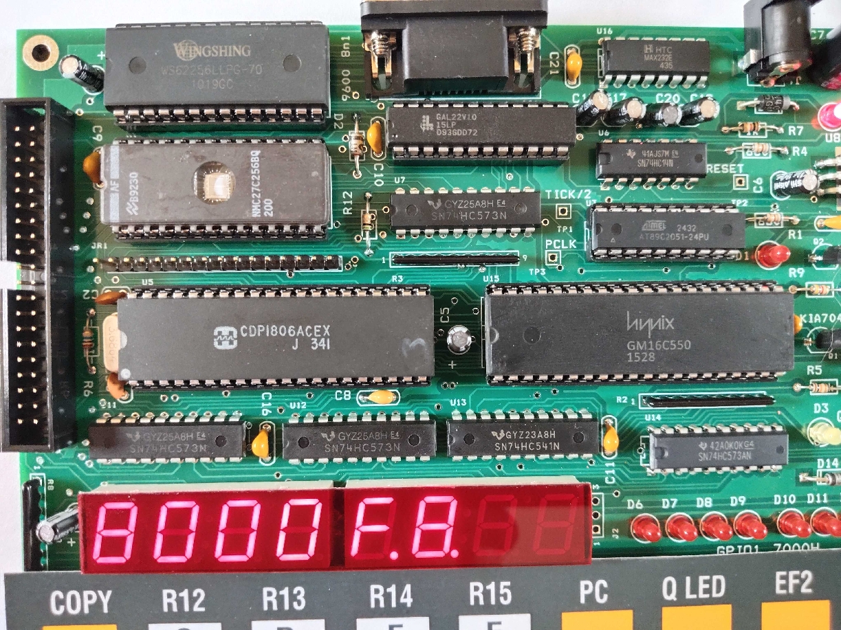
I designed this kit from the suggestion by Leonard Rose. The CDP1802 Microprocessor is very interesting CPU. I use the same platform as the 6809 kit. I spent a month to develop it. The first try PCB was working very good. So most of the time are spent on monitor program coding. The outlook is shown below. The kit runs with Xtal 3.6864MHz using the on chip oscillator. Memory spaces are 28kB monitor ROM, 32kB RAM and 4kB memory mapped I/O. The kit provides 36 keys, 6-digit seven segment display, 9600 UART chip, the 8-bit gpio1 debugging LED, and the text LCD interface. In addition, the 10ms tick generator is also provided for timer interrupt testing. We can enter 1802 instructions with hex code and test run directly. The built-in BREAK subroutine provides CPU registers saving. The expansion header provides interface signals for testing with IN and OUT instructions.
The CDP1802 Microprocessor kit 2018

Hardware descriptions:

U5 is the COSMAC CDP1802 Microprocessor. The CPU clock is generated by the on chip oscillator with external Xtal, 3.6864MHz. The clock signal is also supplied to the tick generator and UART chips. CLEAR pin is used for startup reset by R5-C4 time constant. WAIT signal is pulled up to logic HIGH. On power up, the CPU will start running the monitor program in ROM.

External memory is interfaced with data bus BUS0-BUS7 and A0-A15. A0-A7 emits from MA0-MA7, while the A8-A15 will need external latch, U7 and use TPA signal for latching the high address.

Memory read/write signals for EPROM, SRAM and memory mapped I/O are decoded by U4, the programmable logic device, GAL22V10. See the equations below.

U1 is 32kB EPROM, 27C256. The address space for EPROM is decoded at 0x0000-0x6FFF.

U2 is 32kB static RAM, 62256. The RAM space is located at 0x8000-0xFFFF.

All I/O are decoded to memory locations from 0x7000 to 0x7FFF.

U3, the 20-pin 89C2051 microcontroller chip produces 10ms tick. SW1 selects between 10ms tick or manual INT button.

U13, 74HC541 is 8-bit input port (PORT0). Six bits, PA0-PA5 are input signals of the row keypad. PA6 is for USER test button.

U11, 74HC573 is 8-bit output port (PORT2). The 8-bit output drives the 7-segment LED directly. No current limit resistor. U12 (PORT1) drives 6-digit common cathode pin. The brightness is controlled by software controlled PWM. PC7 is speaker output for beep signal.

U14(GPIO1), 74HC573 is 8-bit output port for 8-bit binary number display.

D14 lifts the forward biasing for proper brightness.

JR1 is 16-pin socket for text LCD interface. Any text LCD with HD44780 compatible controller can be used with no modifications. U16, HIN232 converts TTL level to RS232 level.

U15, is hardware UART using the INS8250 chips. All registers are located in memory space. The input clock signal is the same CPU frequency, 3.6864MHz. To produce 9600 bit/s, we can use internal divider with 24. It will produces 16x9600 Hz exactly.

Q2, KIA7042 is reset chip for power brownout. JP1 is 40 pins header. It is for expansion for testing the IN/OUT instructions.
Hardware schematic (click to enlarge)

Hardware Features:

-CPU: Intersil CDP1802 CMOS Microprocessor @3.6864MHz clock
-Memory: 32kB SRAM, 28kB EPROM, 4kB memory mapped I/O
-Memory and I/O Decoder chip: Programmable Logic Device GAL22V10D
-Display: high brightness 6-digit 7-segment LED
-Keyboard: 36 keys
-RS232 port: INS8250 UART, 9600 bit/s 8n1
-Debugging LED: 8-bit GPIO1 LED at location $7000
-Q LED: high brightness yellow color dot LED for Q output bit
-Tick: 10ms tick produced by 89C2051 for time trigger experiment
-Text LCD interface: direct CPU bus interface text LCD
-Brownout reset: KIA7042 reset chip for power brownout reset
-Expansion header: 40-pin header

The CPU being tested is Intersil CDP1802ACE..

Monitor program was developed using c and assembly language. Source code was compiled with lcc compiler for 1802 CPU. The source code is available for customizing your own monitor.

The monitor program features:

-Simple hex code entering
-Insert and Delete byte
-User registers: D, R3-R15, used for saving CPU registers after BREAK
-Copy block of memory
-Intel HEX file downloading
-Memory dump
-Beep ON/OFF
-TEST 10ms tick

The monitor program will be updated and available for testing at the download links.

Keyboard layout: Making key layout sticker is simply done by printing the SVG file to sticker paper.
Keyboard layout. 

The memory decoder is made with PLD chip, GAL22V10. The equations were compiled to JEDEC file using WInCupL. The locations of memory and I/O devices are shown in the comment lines.

Name     1802KIT ;
PartNo 22V10 ;
Date 3/12/2016 ;
Revision 01 ;
Designer Engineer ;
Company Fangkhao ;
Assembly None ;
Location ;
Device p22v10;
/* *************** INPUT PINS *********************/
PIN 2 = MRD; 
PIN 3 = MWR; 
PIN 4 = A15; 
PIN 5 = A14; 
PIN 6 = A13; 
PIN 7 = A12; 
PIN 8 = A10; 
PIN 9 = A9;
PIN 10 = A8; PIN 11 = A1;
PIN 13 = A0; PIN 1 = TPB;
FIELD ADDRESS = [A15..A12]; 
         
/* *************** OUTPUT PINS *********************/
PIN 14 = OPT; 
PIN 15 = UART; 
PIN 16 = PORT2; 
PIN 17 = PORT1; 
PIN 18 = PORT0; 
PIN 19 = LCD_E;
PIN 20 = GPIO1;
PIN 21 = RAM_WR;
PIN 22 = RAM_CE;
PIN 23 = ROM_CE; 
!ROM_CE = !MRD & ADDRESS:[0000..6FFF];
!RAM_CE = ADDRESS:[8000..FFFF];
!RAM_WR = !MWR & ADDRESS:[8000..FFFF];
!GPIO1 = A15 # !A14 # !A13 # !A12 # A10 # A9 # A8 # A1 # A0 # MWR; /* 7000H */
PORT0 = A15 # !A14 # !A13 # !A12 # A10 # A9 # !A8 # A1 # A0 # MRD; /* 7100H */
!PORT1 = A15 # !A14 # !A13 # !A12 # A10 # A9 # !A8 # A1 # !A0 # MWR; /* 7101H */
         
!PORT2 = A15 # !A14 # !A13 # !A12 # A10 # A9 # !A8 # !A1 # A0 # MWR; /* 7102H */
!LCD_E = A15 # !A14 # !A13 # !A12 # A10 # !A9 # A8 # (MWR & MRD); /* 7200H */
         
UART = A15 # !A14 # !A13 # !A12 # A10 # !A9 # !A8; /* 7300H */

PLD equations 

Example of test code. The assembler format is a18 assembler for 1802 microprocessor.


Simple program that makes Q LED blinking. R3 is used as the pointer to the delay support subroutine.

The delay subroutine is loaded on RESET to the last page of RAM.

The delay uses the low byte of R6 and R7.

We can enter the code only from 8000 to 800B, no need for the delay code.

The monitor program loads the delay code automatically. Then we can press PC then, GO. We will see Q LED blinking. Can you change blinking rate? How?

Another example of using 10ms tick generator for counting binary at 10Hz rate.

R1 is loaded with interrupt vector, R2 is loaded with stack location by monitor program. Test with 10ms tick, by selecting the 10ms tick position on SW1.

On interrupt, the stack (pointed by r2) was decrement by one, the XP bit was saved to stack memory. R6 is used for tick counting. R5 is for gpio1 display. The counting rate is 10Hz.

Can you change from 10Hz to 1Hz counting rate, how?

The kit has 9600 UART, we can dump memory with key DUMP and download Intel HEX file with key LOAD.

To load the hex file, the transmit delay will be needed.

Intel HEX file transfer with 1ms character delay setting.

Any text LCD with HD44780 compatible controller can be used. 

PARTS LIST

Semiconductors

U1 27C256, 32kB EPROM
U2 HM62256B, 32kB SRAM
U3 AT89C2051, programmed 10ms tick generator
U4 22V10, proprogrammed PLD
U5 CDP1802A, CMOS microprocessor
U6 74HC14A
U7,U11,U12,U14 74HC573
U8 7805, +5V voltage regulator
U10,U9 LTC-4727JR, high brightness 7 segment display
U13 74HC541
U15 INS8250, UART
U16 HIN232, RS232 converter

Q1 KIA7042, voltage detector
Q2 BC327, PNP transistor

D1,D6,D7,D8,D9,D10,D11, 3mm LED (red)
D12,D13
D2 1N4733A
D3 Q LED ( yellow)
D4 POWER LED
D5 1N4001
D14 1N5227A

Resistors (all resistors are 1/8W +/-5%)


R4,R1 680
R3,R2 RESISTOR SIP 9
R13,R5 10k
R6 10M
R7 1k
R11,R8 10k RESISTOR SIP 9
R9 4.7k
R10 20
R12 5

Capacitors


C1,C4,C5,C15,C18,C19,C20 10uF
C3,C2 22pF
C6 10uF 16V
C7 1000uF25V
C8,C9,C10,C11,C12 0.1uF
C13,C14 0.1uF
C21,C16 100nF
C17 10uF 10V

Additional parts


JP1 HEADER 20X2
JR1 CONN RECT 16
J1 DC Input
J2 CON3
LS1 SPEAKER
SW2 INTRPT
SW3 RESET
SW4 EF1
SW5 EF2
S1,S2,S3,S4,S5,S6,S7,S8, 12mm tact switch
S9,S10,S11,S12,S13,S14,
S15,S16,S17,S18,S19,S20,
S21,S22,S23,S24,S25,S26,
S27,S28,S29,S30,S31,S32
SW1 ESP switch, 10ms selector switch
VB1 SUB-D 9, Male (cross cable)
Y1 3.6864MHz Xtal
PCB double side plate through hole
display filter sheet, Amber color
Keyboard sticker printable SVG file

Kit is available on ebay. PayPal and Bitcoin are welcome, please contact Wichit Sirichote

Running the kit with smart phone POWER BANK! For outdoor playing, the kit can be powered with power bank. Simply wire the center pin of DC jack to +5V test point. This modification is only for using where no AC power.

CDP 1802 Microprocessor Kit: Review and Demonstration on Youtube

Download Schematic, Monitor source code , lcc42, v1 ROM hex file, PLD files, AT89C2051 HEX file, Keypad SVG file

Quick start
Programming Book rev1.0
Programming Book DOC file, Sample assembly program
User's Manual rev1.0

What's New?

December 13, 2021 Sample program, 16-bit division by Jason M. Zinserling


<

Last updated December, 2021
17 September, 2018